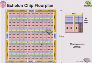
CES 2012 brought in some details about Nvidia’s Echelon supercomputer chip! If we recall, in the middle of 2010, Nvidia disclosed plans for a 20 Teraflop supercomputer named Echelon, within a competition set up by the US Department of Defense. It was competing head-on with Intel and IBM. Details of such a chip have been vague but now some documents presented at Supercomputing 2011 have been put out.
The slideware, obtained from a University of Gent presentation shows a block diagram for a 17mm-by-17mm chip packing 64×4 SM attached to 4-way DRAM I/Os. One can also see the core logic diagrams and SM Lane architecture (8 SM lanes per SM unit) detailed in the presentations. Nvidia also estimates to be able to run these processors at a mild 2.5GHz frequency on a 10nm high-performance node, or 2GHz in the low-power version, and is aiming at 4x power savings over current 40nm designs.
Nvidia’s preferred foundry partner’s plans, TSMC, had previously announced that 10nm would be possible in the 2017/2018 time frame, at best, which is in line with the presentation projections. Nvidia will face-off with Intel’s “Knights Landing” 2nd generation supercomputer chip in that time frame.
, nvidia super computer
